

Photolithography Machine
Your Professional Photolithography Machine Supplier!
EO EQUIPMENT is a global supplier of high-quality industrial machinery and equipment, providing comprehensive solutions across construction, cleaning, machine tools, food processing, and packaging sectors. Backed by over 20 years of sourcing and export experience, we connect international buyers with trusted Chinese manufacturers to deliver efficient, customized solutions.


Specification
|
Specification |
Details |
|
Machine Type |
Photolithography Machine |
|
Exposure Method |
UV Light Exposure (LED or Mercury vapour) |
|
Exposure Area |
600 × 700 mm – 5000 × 1200 mm (model dependent) |
|
Resolution / Precision |
Typically 50–100 µm or better |
|
Alignment System |
Automatic or manual alignment systems |
|
Light Source |
UV LED or traditional UV lamps |
|
Control System |
PLC or computer-controlled interface |
|
Power Supply |
Standard industrial voltage (e.g., 380 V / 220 V) |
|
Cooling System |
Forced air or water cooling |
|
Machine Dimensions |
Varies by model and working size |
|
Machine Weight |
Approx. 800–3000 kg (varies by model) |
|
Construction Material |
Industrial-grade steel frame |
|
Applicable Substrate |
PCB panels and dry film panels |

High-Quality Patterns: Photolithography machine creates precise and detailed patterns on various surfaces like computer chips.
Efficient Production: It's effective in mass production, like production of computer chips in a factory.
Cost-Effective: It is relatively affordable to make more items, after the initial setup.
Versatile: It can be used with different materials, including metals and plastics.
Accurate Alignment: It ensures that all parts fit together correctly.
Fast Processing: It enhances the pace of machine working which increases production speed.
Light Source: Generates the light used for pattern transfer.
Optical System: Focuses and directs the light onto the wafer.
Photomask: Contains the pattern to be transferred.
Stage: Holds and moves the wafer during the lithography process.
Alignment System: Ensures precise positioning of the wafer and photomask.

Patterning:
Photolithography machine is based on transferring a specific pattern from a photomask to a substrate, usually a semiconductor wafer. This pattern forms the basis of electronic circuits.
Application of photoresist:
Photoresist, which is a light-sensitive material, is uniformly applied to the substrate. When exposed to light, the photoresist undergoes chemical changes that are necessary to create the pattern on the substrate.
Exposure and development:
A substrate coated with photoresist is exposed to light (e.g., ultraviolet light) through a photomask that bears the desired pattern. The light changes the solubility of the photoresist. The substrate is then developed by washing away either exposed or unexposed areas of photoresist, depending on whether positive or negative photoresist is used.
Etching:
After developing, the exposed areas of the substrate from which the photoresist has been removed are etched away, usually with chemicals or plasma. As a result, the pattern is imprinted into the substrate.
Removing the remaining photoresist:
The remaining photoresist is removed, leaving the substrate with the pattern ready for further processing.
Types of Photolithography Machine
Photolithography
Uses light to transfer a pattern from a photomask to a light-sensitive photoresist on the wafer surface.
Electron Beam Lithography
Uses a focused beam of electrons to write patterns directly onto the wafer, offering higher resolution than photolithography.
Extreme Ultraviolet (EUV) Lithography
Uses extreme ultraviolet light with shorter wavelengths to achieve even finer pattern resolutions.
Applications of Photolithography Machine
In semiconductor manufacturing, photolithography machines are indispensable. They enable the production of microprocessors, memory chips, and sensors. For example, advanced EUV lithography tools are used to produce 7nm and smaller nodes, pushing the limits of miniaturization.
Display manufacturing also relies on lithography for creating thin, high-resolution screens in smartphones and TVs. The technology ensures precise patterning of OLED and LCD panels, resulting in sharper images and better color accuracy.
In the realm of MEMS, lithography is used to produce tiny mechanical devices integrated with electronics, such as accelerometers in smartphones or medical sensors. These applications demand high precision and repeatability, which photolithography machines provide.
Nanotechnology research benefits from lithography by enabling the creation of nanostructures for scientific experiments, advanced materials, and novel devices. The ability to pattern at nanometer scales opens new frontiers in science and engineering.
Customized Services
To better meet the diverse needs of different industries and clients, we can customize professional construction machinery solutions based on your specific application scenarios and special requirements. For further information or support, please feel free to contact us.

- Contact Customer Service
- Submit Order
- Obtain a Quote
- Confirm Order
- Arrange Payment
- Track Order
- Receive and Inspect Goods
Packaging
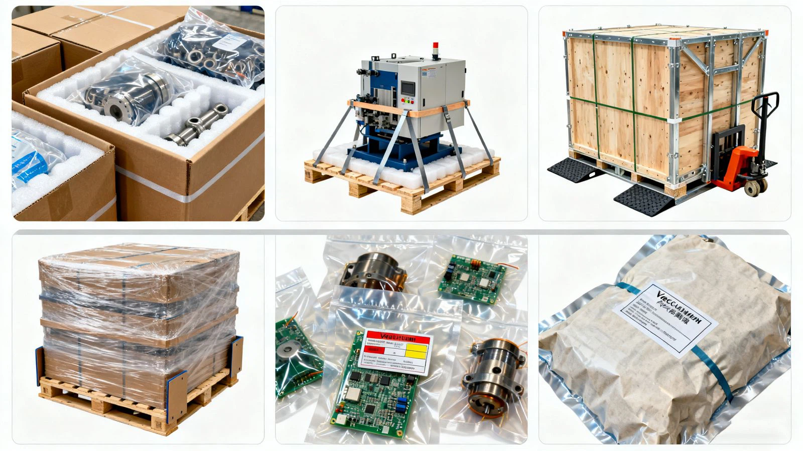
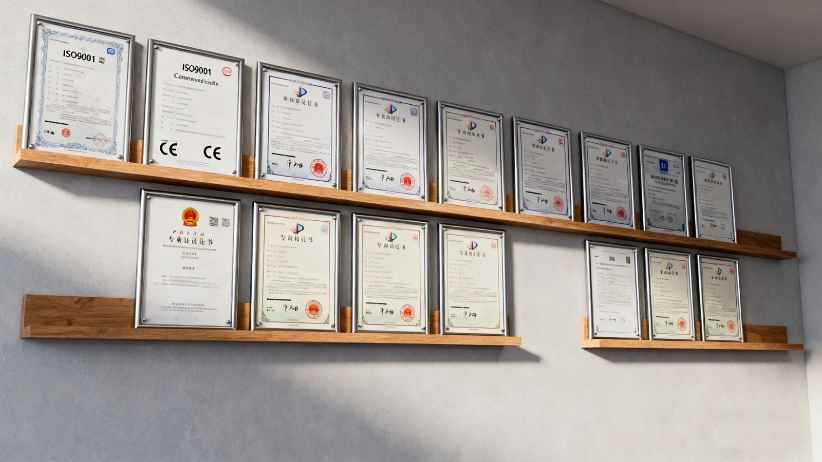
Our Certificate
FAQ
As one of the most reliable photolithography machine manufacturers and suppliers in China, we offer a wide range of products with superior quality. Please rest assured to buy high-grade photolithography machine made in China here from our factory. Browse our website now.
Inner Outer Layer PCB Lithography Machine, PCB Lithography Machine, Solder Mask PCB Alignment Machine